3.2. Switching controller subsystem
Contents
3.2.1. Introduction

The switching controller is the block that compares the modulating (or reference) waveform and carriers in order to generate Pulse-Width-Modulated (PWM) control signals. These signals are then used to control which switch is turned on in each cell of the macrocells of the conversion stage.
3.2.2. Inputs and outputs of the subsystem configuration interface
3.2.2.1. User-defined parameters
3.2.2.1.1. fsw
Switching frequency of each power switch.
Warning
In a DC/AC conversion stage, the switching frequency fsw must be a multiple of the AC frequency. This limitation is due to the way the PowerForge solving engine operates and might be lifted in the future.
3.2.2.1.2. Carrier type
This section only applies to DC/AC conversion stages.
To determines the shape of the carrier waveform. For now, only triangle is available.
3.2.2.1.3. Sample type
This section only applies to DC/AC conversion stages.
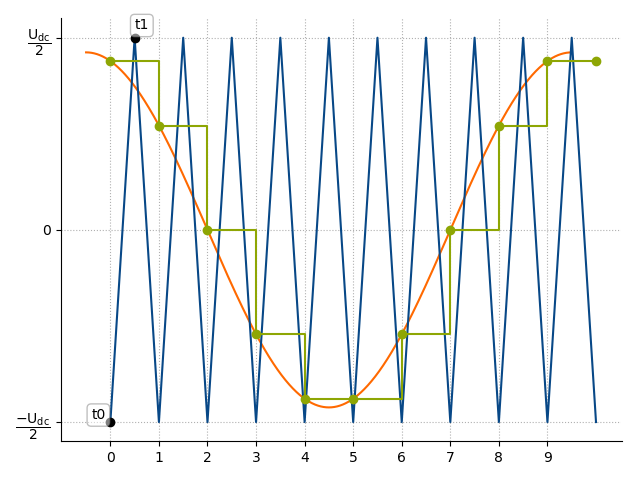
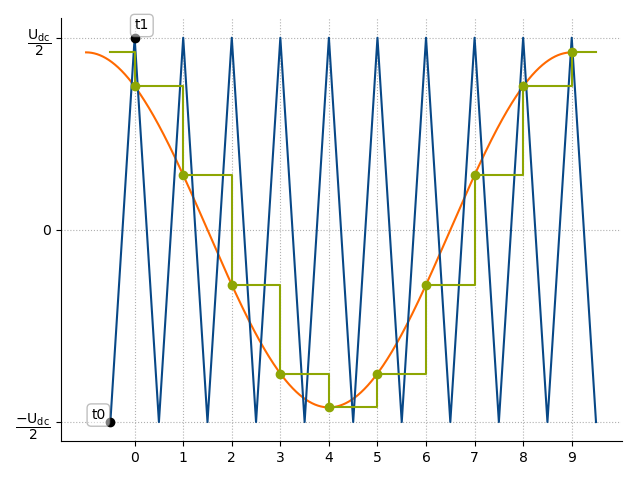
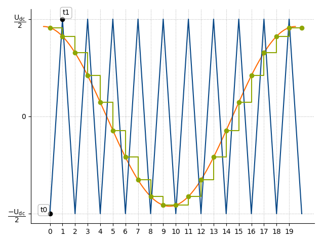
To avoid over-switching, the reference waveform is sampled/held at certain instants in the carrier period.
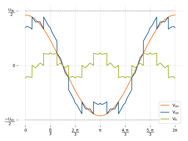
t0: the reference waveform is blocked at each valley of the carrier waveform.
t1: the reference waveform is blocked at each peak of the carrier waveform.
Sample at both t0 & t1: the reference waveform is blocked at each valley and peak of the carrier waveform.
t0 |
t1 |
both t0 & t1 |
3.2.2.1.4. Carrier disposition
This section only applies to 3-phase DC/AC conversion stages.
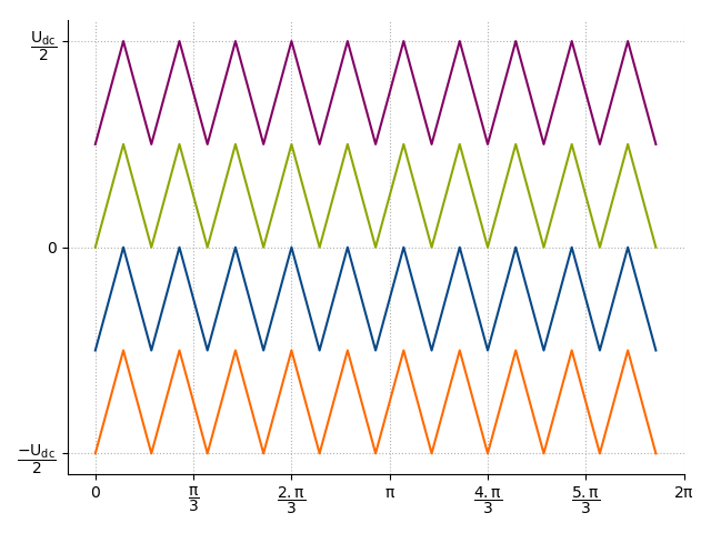
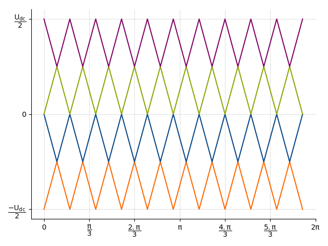
To determine the different “levels” of the macrocell, several carrier waveforms are stacked in the modulator.
Phase Disposition (PD): all the different carriers are synchronised and have the same phases.
Alternate Phase Opposition Disposition (APOD): consecutive carriers are shifted by 180°.
PD |
APOD |
3.2.2.1.5. Inverter gain
This section only applies to DC/AC conversion stages.
The inverter gain \(\mathbf{G}\) is the ratio between the AC phase-to-phase fundamental rms voltage \(\mathbf{U_{AC,0}}\) and half the DC bus voltage \(\mathbf{U_{DC}}\)
Depending on the inverter topology, the gain \(\mathbf{G}\) is expressed as follows:
Three-phase inverter:
Single phase inverter:
3.2.2.1.6. Modulation depth
This section only applies to DC/AC conversion stages.
The modulation depth \(\mathbf{M}\) is the amplitude of the sine reference and homopolar signals.
The phase to neutral voltage (reference signal scaled to the DC bus voltage) is expressed as follows:
3.2.2.1.7. Modulation operating region
This section only applies to DC/AC conversion stages.
The value of the modulation depth determines whether Linear or Over Modulation is used.
In Linear Modulation region, the relationship between the inverter gain and the modulation depth is purely linear: \(\mathbf{G(M) = M}\).
In Over Modulation region, the relationship between the inverter gain and the modulation depth is non-linear \(\mathbf{G(M) = f(M)}\), where the relationship depends on the modulation strategy.
Note
The linearity limit for the Sine modulation strategy is reached for a maximum modulation depth \(M\) equal to \(1\). For all the other modulation strategies which add a third harmonic component, the maximum modulation depth \(M\) for linearity is equal to \(2/\sqrt{3} \approx 1.15\). If the modulation depth exceeds these limits, over modulation is used.
3.2.2.1.8. Modulation strategy - Linear Modulation (LM)
This section only applies to 3-phase DC/AC conversion stages.
If the neutral point of the AC bus is floating, a homopolar reference can be inserted to boost the output voltage range or reduce the switching losses.
The phase-mid point voltage can be expressed as the sum of the phase neutral voltage and a homopolar component:
The expression of the homopolar voltage depends on the chosen modulation strategy.
The modulation strategies are divided in two groups:
Continuous modulation strategies
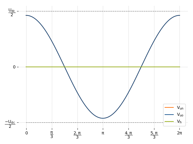
- Sine PWM
With this modulation strategy, there isn’t any homopolar voltage. This is the simplest modulation strategy.
\[V_h = 0\]
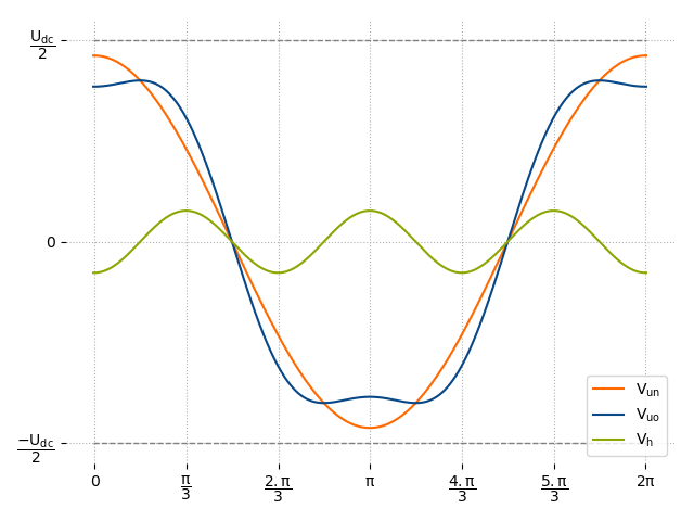
- 3rd harmonic injection
This method 1 adds a sinusoidal homopolar voltage at 3 times the fundamental frequency. It allows increasing the phase-neutral voltage up to \(U_{DC}/\sqrt{3}\).
\[V_h = \frac{U_{DC}}{2} \left( -\frac{M}{6} \sin{3\omega_{0}t} \right)\]
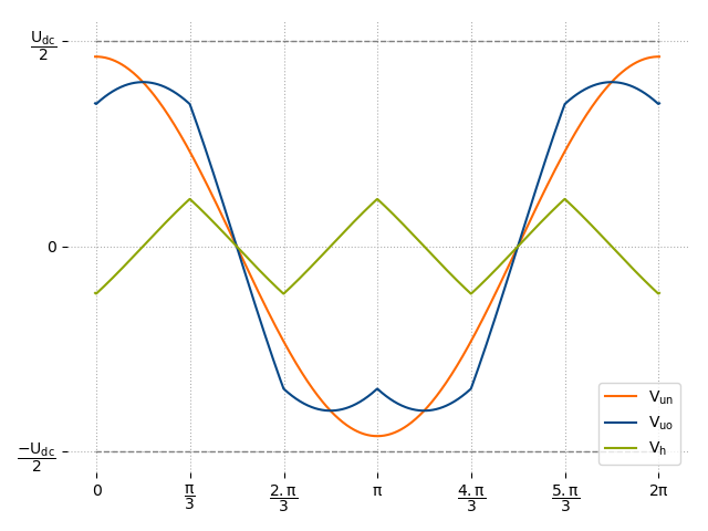
- Space vector
This method 2 gives the lowest harmonic distortion for a two-level converter.
\[V_h = - \frac{max(V_{UN}, V_{VN}, V_{WN}) + min(V_{UN}, V_{VN}, V_{WN})}{2}\]
- Multilevel Space vector
This method 3 4 is an adaptation of the Space vector modulation for the specific case of multilevel converters.
\[V_{off} = - \frac{max(V_{UN}, V_{VN}, V_{WN}) + min(V_{UN}, V_{VN}, V_{WN})}{2}\]\[V'_{kN} = \left(V_{kN} + V_{off} + \frac{U_{DC}}{2} \right) \mod \left( \frac{U_{DC}}{N - 1}\right) \:\:\: k=\left\{U, V, W\right\}\]\[V'_{off} = \frac{U_{DC}}{2\left(N-1\right)} - \frac{max(V'_{UN}, V'_{VN}, V'_{WN}) + min(V'_{UN}, V'_{VN}, V'_{WN})}{2}\]\[V_h = V_{off} + V'_{off}\]
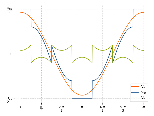
Sine PWM |
3rd harmonic injection |
Space vector |
Multilevel Space vector (N=3) |
Multilevel Space vector (N=4) |
Multilevel Space vector (N=5) |
Discontinuous modulation strategies
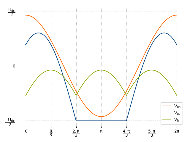
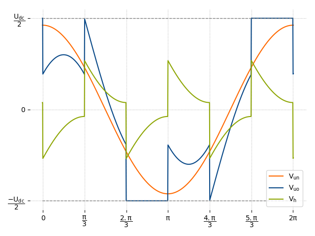
- 120° DPWM DC- clamp
In this strategy, each phase does not switch within 120° of the fundamental period and the output is clamped at the negative dc bus voltage 5. As consequence, the switches connected to the negative dc bus voltage reduce their switching losses.
\[V_h = -\frac{U_{DC}}{2} - min(V_{UN}, V_{VN}, V_{WN})\]
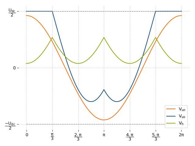
- 120° DPWM DC+ clamp
In this strategy, each phase does not switch within 120° of the fundamental period and the output is clamped at the positive dc bus voltage 5. As consequence, the switches connected to the positive dc bus voltage reduce their switching losses.
\[V_h = \frac{U_{DC}}{2} - max(V_{UN}, V_{VN}, V_{WN})\]
- 60° DPWM centered
In this strategy, each leg does not switch within 60° of the fundamental half-period. This strategy has minimum switching losses for unitary power factor 6. The homopolar component is obtained with the following equations where the angle \(\psi = 0\).
\[V_h = \frac{U_{DC}}{2} sign \left( V_{max} \right) - V_{max}\]\[V'_{kN} = \frac{U_{DC}}{2} M \sin\left(\omega_{0}t + \varphi + \psi \right) \:\:\: \varphi=\left\{ 0, \frac{-2\pi}{3}, \frac{-4\pi}{3} \right\} \:\:\: k=\left\{U, V, W\right\}\]\[\begin{split}V_{max} = \left\{ \begin{array}{ll} V_{UN} & if \: \left|V'_{UN}\right| \ge \left|V'_{VN}\right|, \left|V'_{WN}\right|\\ V_{VN} & if \: \left|V'_{VN}\right| \ge \left|V'_{UN}\right|, \left|V'_{WN}\right|\\ V_{WN} & if \: \left|V'_{WN}\right| \ge \left|V'_{UN}\right|, \left|V'_{VN}\right|\\ \end{array} \right.\end{split}\]
- 60° DPWM leading 30°
It is the same as the DPWM 60° centered except that the angle \(\psi=+\frac{\pi}{6}\). This strategy has minimum switching losses for 30° leading power factor 7.
- 60° DPWM lagging 30°
It is the same as the DPWM 60° centered except that the angle \(\psi=-\frac{\pi}{6}\). This strategy has minimum switching losses for 30° lagging power factor 7.
- 30° DPWM
In this case the phase leg is clamped 30° symmetricaly from maximal voltage. This method has low harmonic distortion characteristics 8. The homopolar component is extracted from the following equations.
\[V_h = \frac{U_{DC}}{2} sign \left( V_{max} \right) - V_{max}\]\[\begin{split}V_{max} = \left\{ \begin{array}{ll} V_{UN} & if \: \left|V_{VN}\right| \ge \left|\mathbf{V_{UN}}\right| \ge \left|V_{WN}\right| \: or \left|V_{WN}\right| \ge \left|\mathbf{V_{UN}}\right| \ge \left|V_{VN}\right|\\ V_{VN} & if \: \left|V_{UN}\right| \ge \left|\mathbf{V_{VN}}\right| \ge \left|V_{WN}\right| \: or \left|V_{WN}\right| \ge \left|\mathbf{V_{VN}}\right| \ge \left|V_{WN}\right|\\ V_{WN} & if \: \left|V_{UN}\right| \ge \left|\mathbf{V_{WN}}\right| \ge \left|V_{VN}\right| \: or \left|V_{VN}\right| \ge \left|\mathbf{V_{WN}}\right| \ge \left|V_{UN}\right|\\ \end{array} \right.\end{split}\]
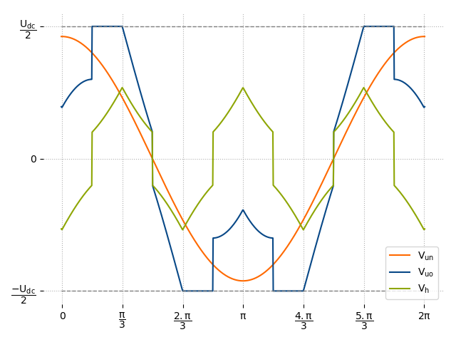
120° DPWM DC- clamp |
120° DPWM DC+ clamp |
60° DPWM leading 30° |
60° DPWM centered |
60° DPWM lagging 30° |
30° DPWM |
The following table resumes the modulation strategies and the macrocell topologies that are compatible. ( ✓ = compatible, ✗ = not compatible, ~ = compatible depending on the case) :
Modulation |
Two-level |
Flying Capacitor |
NPC |
T-Type |
SMC |
Sine PWM |
✓ |
✓ |
✓ |
✓ |
✓ |
3rd harmonic injection |
✓ |
✓ |
✓ |
✓ |
✓ |
Space vector |
✓ |
✓ |
✓ |
✓ |
✓ |
Multilevel Space vector |
✓ |
✓ |
✓ |
✓ |
✓ |
120° DPWM DC- clamp |
✓ |
~ |
✗ |
✗ |
✗ |
120° DPWM DC+ clamp |
✓ |
~ |
✗ |
✗ |
✗ |
60° DPWM leading 30° |
✓ |
~ |
✓ |
✓ |
~ |
60° DPWM centered |
✓ |
~ |
✓ |
✓ |
~ |
60° DPWM lagging 30° |
✓ |
~ |
✓ |
✓ |
~ |
30° DPWM |
✓ |
~ |
✓ |
✓ |
~ |
3.2.2.1.9. Modulation strategy - Over Modulation (OM)
This section only applies to 3-phase DC/AC conversion stages.
As mentioned in a previous section, the over modulation region is reached if modulation depth \(M\) exceeds the linearity limit.
Some modulation strategies allow for over modulation, which users can identify by the acronym OM in the choices offered:
Sine PWM OM
3rd harmonic injection OM
Space vector OM
60° DPWM leading/lagging 30° OM
60° DPWM centered OM
Over modulation allows the user to further increase the inverter gain \(G\), and ultimately, the AC voltage \(U_{AC,0}\) 8, by increasing the modulation depth \(M\) over the linearity limit.
The theoretical limit, commonly called Six-Step, is reached when \(M \rightarrow \infty\), regardless of the modulation strategy chosen. This specific behavior enables the maximum gain \(G_{SIX-STEP}\) for a 3-phase DC/AC converter:
When the modulation depth \(M\) is between the point of maximum linearity and Six-Step operation, the inverter gain \(G\) is a nonlinear function of the modulation depth. The function used depends on the modulation strategy chosen.
The following figure is an example of a Sine PWM modulation strategy with a modulation depth of \(M = 1.2\).
In order to obtain the right modulation depth for a target AC voltage, the following equations are used 8:
Modulation strategy |
Condition |
Formula |
|---|---|---|
Sine PWM OM |
\(\forall M\) |
\(G = \frac{2}{\pi}\times M\times \arcsin\bigg(\frac{1}{M}\bigg) + \frac{2}{\pi}\times \sqrt{1 - \frac{1}{M^2}}\) |
3rd harmonic injection OM |
\(M < 6/5\) |
\(G = \frac{2}{\pi}\times M\times \bigg( \alpha_1-\alpha_2 +\frac{5}{12}\big(\sin(2\alpha_1) - \sin(2\alpha_2)\big) +\frac{1}{24}\big(\sin(4\alpha_1) - \sin(4\alpha_2)\big) \bigg) +\frac{4}{\pi}\times\big(\cos(\alpha_1) - cos(\alpha_2)\big)\) |
\(M \geq 6/5\) |
\(G = \frac{2}{\pi}\times M\times \bigg( \alpha_1 +\frac{5}{12}\sin(2\alpha_1) +\frac{1}{24}\sin(4\alpha_1) \bigg) +\frac{4}{\pi}\times\cos(\alpha_1)\) |
|
With \(\sin(\alpha_{1,2}) + \frac{1}{6}\sin(3\alpha_{1,2}) = \frac{1}{M}\) |
||
Space vector OM |
\(M < 4/3\) |
\(G = -\frac{1}{2}\times M + \frac{3}{\pi}\times M\times\arcsin\bigg(\frac{2}{\sqrt{3}\times M}\bigg) +\frac{2\sqrt{3}}{\pi}\times\sqrt{1 - \bigg(\frac{2}{\sqrt{3}\times M} \bigg)^2}\) |
\(M \geq 4/3\) |
\(G = \frac{3}{\pi}\times M\times\arcsin\bigg(\frac{2}{3\times M}\bigg) +\frac{2}{\pi}\times\sqrt{1 - \bigg(\frac{2}{3\times M} \bigg)^2}\) |
|
60° DPWM centered OM |
\(M < 4/\sqrt{3}\) |
\(G = -\frac{4}{\pi} + M\times \bigg(\frac{\sqrt{3}}{\pi}-\frac{1}{2}\bigg) + \frac{4}{\pi\sqrt{3}\times M} + \frac{3}{\pi}\times M\times\arcsin\bigg(\frac{2}{\sqrt{3}\times M}\bigg) + \frac{2\sqrt{3}}{\pi}\times\sqrt{1 - \bigg(\frac{2}{\sqrt{3}\times M}\bigg)^2}\) |
\(M \geq 4/\sqrt{3}\) |
\(G = \frac{4}{\pi}\) |
|
60° DPWM leading/lagging 30° OM |
\(M < 4/3\) |
\(\begin{matrix} \ a_1= & \frac{\pi}{16}\times M - \frac{\sqrt{3}}{2}\sin\big(\psi-\frac{\pi}{6}\big) + \frac{3\psi\times M}{8} - \frac{3}{16}\times M\cos\big(2\psi+\frac{\pi}{6}\big)\\ \\\ \ b_1= & -\frac{1}{2}\cos\big(\psi + \frac{\pi}{3}\big) + \frac{\sqrt{3}}{16}\times M\bigg(\frac{\pi}{3}-2\psi-\sin\big(2\psi-\frac{\pi}{3}\big)\bigg) \end{matrix}\) |
\(M \geq 4/3\) |
\(\begin{matrix} \ \alpha= & \frac{2\pi}{3} - \arcsin\big(\frac{2}{\sqrt{3}\times M}\big)\\ \\\ \ a_1= & \frac{\sin\alpha}{2} + M\times\bigg(\frac{1}{2} - \frac{\sqrt{3}}{8\pi} - \frac{3\alpha}{4\pi}\bigg)\times\frac{\pi}{4} - \frac{\sqrt{3}}{16}\times M\cos\big(2\alpha - \frac{2\pi}{3}\big)\\ \\\ \ b_1= & -\frac{\cos\alpha}{2} + \frac{\sqrt{3}}{8}\times M\bigg(\frac{\sqrt{3}}{4}-\frac{1}{2}\sin\big(2\alpha-\frac{2\pi}{3}\big) + \frac{\pi}{3} - \frac{\alpha}{2}\bigg) \end{matrix}\) |
|
With \(\left\{\begin{matrix} \psi= & -\frac{\pi}{3}+\arcsin{\frac{\pi}{2\sqrt{3}\times M}}\\ \\\ \ G= & \frac{8}{\pi}\times\sqrt{a_1^2 + b_1^2} \end{matrix}\right.\) |
||
The following figure illustrates the different inverter gain equations expressed in the previous table:
Warning
It is important to note that if the ratio of the switching frequency \(f_{sw}\) to the target fundamental AC frequency \(f_{0}\) is below or close to 20, it becomes possible to obtain designs where the inverter gain is greater than the limit of \(4/\pi\). Care should be taken when considering this ratio.
3.2.2.2. Waveforms
3.2.2.2.1. Comparator waveforms
The carrier and reference waveforms compared internally by the modulator to generate the control signals are displayed on this graph.
3.2.2.3. Over modulation case study
To illustrate the interest of using over modulation, let’s take an example of a 3-phase DC/AC converter with a machine with MTPA + FW controller.
The modulation strategy applied to this example is the Space vector with and without the ability to behave in over modulation.
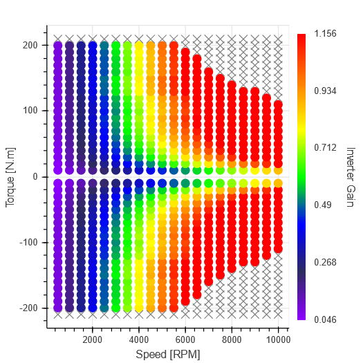
Inverter gain comparison:
Only Linear Modulation allowed |
Both Linear and Over Modulation allowed |
|---|---|
|
|
By allowing for over modulation, higher inverter gains in the FW region can be achieved as compared to when only linear modulation is used. As a reminder, inverter gain greater than \(2/\sqrt{3} \approx 1.15\) typically requires the use of over modulation for a Space vector modulation strategy.
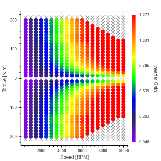
AC Voltage comparison:
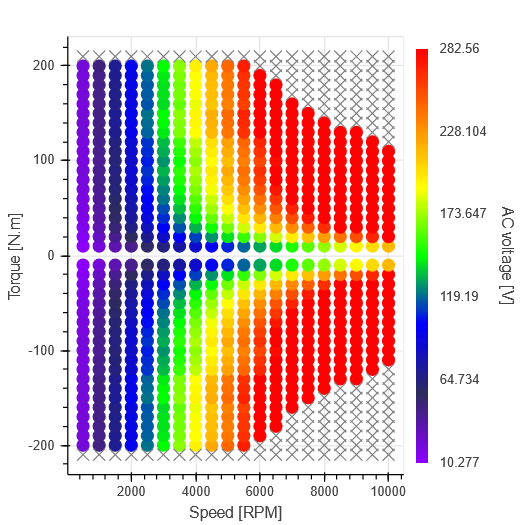
Only Linear Modulation allowed |
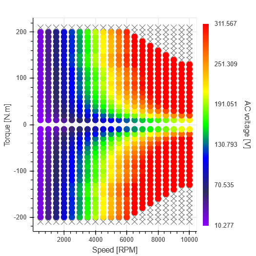
Both Linear and Over Modulation allowed |
|---|---|
|
|
This higher inverter gain leads to higher AC voltage also in FW region.
Switching losses comparison:
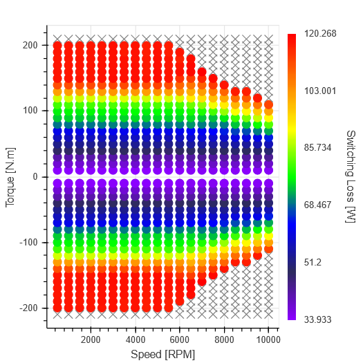
Only Linear Modulation allowed |
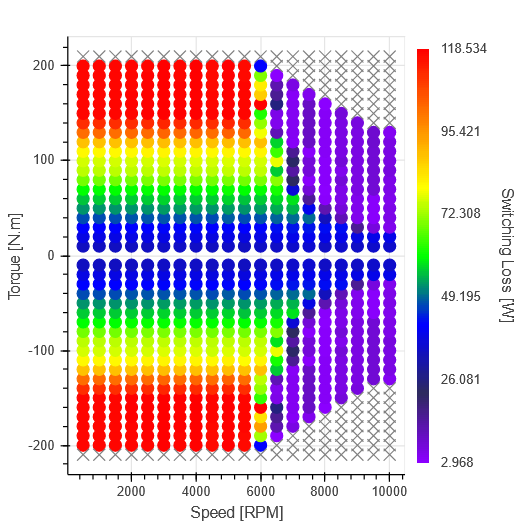
Both Linear and Over Modulation allowed |
|---|---|
|
|
Due to the behavior becoming closer to that of a Six-Step, switching losses are significantly reduced in the FW region.
3.2.2.4. Citations
- 1
G.Buja and G. Indri. “Improvement of pulse width modulation techniques”. Archiv fur Elektrotechnik, 57, pages 281-289, 1975.
- 2
H.W. van der Broeck, H. Skudelny and G.V. Stanke, “Analysis and realization of a pulsewidth modulator based on voltage space vectors,” in IEEE Transactions on Industry Applications, vol. 24, no. 1, pp. 142-150, Jan.-Feb. 1988.
- 3
B.P. McGrath, D.G. Holmes and T. Lipo, “Optimized space vector switching sequences for multilevel inverters,” in IEEE Transactions on Power Electronics, vol. 18, no. 6, pp. 1293-1301, Nov. 2003.
- 4
D.G. Holmes, and A. L. Thomas. “Pulse width modulation for power converters: principles and practice”. Vol. 18. John Wiley & Sons, 2003.
- 5(1,2)
K.Taniguchi, Y. Ogino and H. Irie, “PWM technique for power MOSFET inverter,” in IEEE Transactions on Power Electronics, vol. 3, no. 3, pp. 328-334, July 1988.
- 6
M.Depenbrock, “Pulse width control of a 3-phase inverter with non-sinusoidal phase voltages.” Conf. Record of IEEE/IAS Annu. Meeting. 1977.
- 7(1,2)
J.W. Kolar, H. Ertl and F.C. Zach, “Influence of the modulation method on the conduction and switching losses of a PWM converter system,” in IEEE Transactions on Industry Applications, vol. 27, no. 6, pp. 1063-1075, Nov.-Dec. 1991.
- 8(1,2,3)
A.M.Hava, “Carrier based PWM-VSI drives in the overmodulation region”. Vol. 1. University of Wisconsin–Madison, 1998.
